


![]()
Creating PCBs with the toner transfer method
There are many webpages explaining how to create printed circuit boards (PCBs) without having to use UV light and photoresist. However, most of them are bloated, unsurveyable or incomplete. This page is an attempt to document the process in a concise way. If you want to have more details, this may be a good place to look.
- Requirements
- Creating the design
- Printing the design
- Preparing the PCB
- Performing the actual toner transfer
- Removing the paper
- Etching
- Finishing
- Gallery
Requirements
- A blank PCB, without a photoresist layer. If you only have boards with such a layer, you need to remove it first with a solvent like acetone.
- A type of paper, coated with a thin wax-like layer on one side, and easily dissolvable in water. Most inkjet 'photo-paper' is good. Some are better than others. Some companies like PulsarProFX produce special toner-transfer paper which has a kind of sugar-based coating. The toner sticks to this coating, which dissolves completely when soaked in water. The result is a very clean transfer that can also be used to transfer colour laser prints onto various surfaces. The method can also be extended to produce decals that will stick to about any surface, even curved. However, this paper is pretty expensive and hard to get outside the US.
- A laser printer with ordinary toner, 600dpi is recommended.
- A clothes iron.
- Acetone.
- A kind of abrasive sponge, like a scotchbrite pad, or steel wool. Some people say that steel wool may contaminate the copper, but others have used it without problems.
- Paper towel
- A toothbrush or similar semi-soft brush
- An etchant. The traditional etchant for copper is Ferric Chloride, but a cheap and very good alternative is a mixture of Hydrogen Chloride (HCl) and Hydrogen Peroxide (H2O2). Contrary to FeCl3, it's completely transparent, and very cheap (depending on where you get the chemicals).
- Safety goggles and gloves.
Method
Creating the design
 Your final PCB design should consist of a mirrored black-and-white bitmap of the copper pattern of the bottom of the PCB. This can be made in any way, ranging from the output from an expensive professional program to something you draw in the GIMP. A 300dpi image will do fine, anything above 600dpi is overkill.
Strictly spoken, holes are not necessary because you'll drill them anyway, but small holes in your design will make drilling a lot easier, first because you can see where to drill and second because the small hole in the copper will 'guide' the drill when biting into in the PCB. For this last effect to work, you should keep holes small, I use a diameter of 1/60" (0.42mm or 5 pixels in a 300dpi image).
Speaking about holes, if you're going to drill them manually, try to align as many holes on the same lines parallel with the edges of the PCB as possible. This will make it a lot easier and faster to drill them with a drill press, if it has a guide system (improvised or built-in).
Theoretically, everything you can print in a 300dpi image can end up as a copper trace, pad or letter on your print. In practice, anything thinner than 2/300 inch (2 pixels in a 300dpi image) can be problematic. Avoid using 1/300 inch lines or spacings for structures that are supposed to conduct electricity.
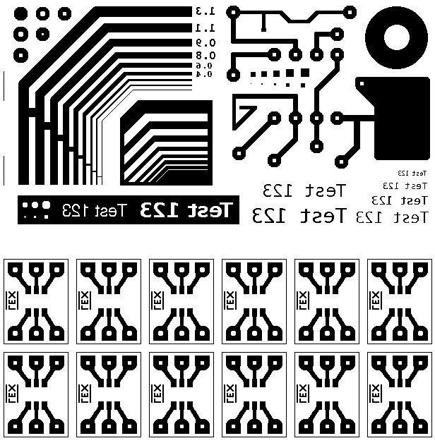
1/300 inch lines may actually work if you keep them away from the edges of the PCB. As a general rule, either avoid putting any fine structures near the edges, or cut the PCB to a size slightly larger than required for the design (and saw off the redundant parts after the transfer). This is because it's harder to properly transfer the toner near the edges. Fine edges may smear, and/or not stick. You can see this below in the photos of the test PCB I made, of which the design is shown at the right.
If you're going to create a double-sided PCB, you will need to include some reference points that match on both sides. It's a good idea to include the edges of the PCB, but you may also put some extra marks outside the PCB area. This will make it easier to verify that the patterns are still aligned once you have sandwiched the PCB between them. You can slightly reduce the need for perfect alignment, by making the 'via' solder pads of one of the sides slightly larger and not drawing drill holes in them.
Printing the design
Read More and see Detailed Instructions...http://www.dr-lex.be/hardware/tonertransfer.html
Dr. Lex' Site
- About: about me and this site.
- Educative Stuff: various stuff you may learn something from.
- Hardware: hardware-related things I've done, including my hand-built electric guitars.
- Software & Sound: software for Mac OS (mostly), but also some sounds, fonts and scripts.
- Weird Stuff: what the title says. Enter at your own risk.
- Links: links to other sites.
Other potentially useful pages: the sitemap and the contact page.
Great info and well written instructions. I will want to come back to this one, when I get around to making my own PCB...
Don
No comments:
Post a Comment